
Parameters:
Applications
1. SEM: The morphology observation and analysis of various materials, such as metals, semiconductors, ceramics, polymer materials, organic polymers
2. EDS: The micro area composition analysis of the materials
3. EBSD: Crystal orientation and texture analysis and 3D reconstruction of polycrystalline materials
4. FIB: Preparation of the micro and nanostructure, including TEM and APT sample preparation under SEM on-line observation, material micro cross section interception and observation, material micro etching and deposition, etc.
Features
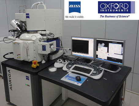
Zeiss Auriga focused ion beam / field emission scanning double-beam electron microscopy (FIB) is an international advanced equipment for the analysis of nanostructures and preparation of micro-nano structures. It is equipped with electron beam and Ga ion beam, which can realize the simultaneous on-line observation with electron beam and ion beam. The device has the characteristics of stable beam flow, high resolution and accurate nanometer manipulation. It can be used for TEM and APT sample preparation. It also can be used to observe and analyze the microstructure, crystal structure and phase structure of the materials under the resolution of nanometer scale, as well as qualitative and quantitative detection of chemical components in various material micro regions.
Parameters
SEM Resolution: 1.0nm @ 15kV, 1.9nm @ 1 kV
Mag.:12 ~ 1000,000
EHT: 0.1 ~ 30 kV
FIB Resolution: 2.5 nm @ 30kV
Magnification: 300× ~ 500,000×
EHT: 1.0 ~ 30 kV
X-ray spectrometer
Resolution: 127 eV @ MnKα
Detection range of elements: Be (4) ~ Fm (100)
EBSD Detector
Spatial resolution: 50nm
Address: Main Building-165
Contact: Qiao Yi, Chen Xiaohua
Tel: 62332634 (Lab) 62333502 (Qiao) 82375388 (Chen)