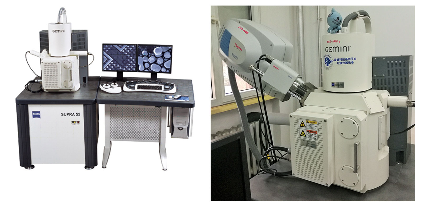
Parameters:
Applications
SUPRA55 thermal field emission scanning electron microscope is widely used in the observation and analysis of material morphology in metallurgy, biology, construction, machinery and other industries, such as metals, semiconductors, ceramics, polymer materials, organic polymers. The electron microscope is equipped with an X-ray energy spectrum analyzer and an EBSD backscattered electron orientation imaging system. EBSD is an important tool for characterization of materials. It can display the crystal orientation and texture of polycrystalline materials in the form of crystal orientation maps.
Features
SUPRATM 55 adopts the patented GEMINI tube design and ring-shaped IN-LENS SE detector. It has the characteristics of stable beam and high resolution. It can perform high-resolution imaging and elemental composition analysis of conductive samples and non-conductive samples at the same time.
1. Schottky (Schottky) field emission electron source with large emission current and high stability
2. The patented technology GEMINI lens barrel is used to overcome the shortcomings of the traditional unipolar objective diaphragm design and eliminate the magnetic effect. At the same time, the cross-optics-free design is adopted to improve the main performance of the instrument.
3. Beam booster (electron beam accelerator) is used to get excellent low acceleration voltage performance
4. Ring efficient In-lens SE detector with good resolution and symmetry
5. Electromagnetic/electrostatic composite objective lens for high-resolution imaging of magnetic substances
Parameters
Detector: Inlens secondary electron detector
E-T secondary electron detector
4Q BSD backscattered electron detector
X-ray spectrometer
Resolution: 132 eV @ MnKα
Detecting element range: Be (4) ~ Fm (100)
Resolution: 1.0 nm @ 15 kV, 1.7 nm @ 1 kV, 4.0 nm @ 0.1 kV
Magnification: 12 ~ 900,000×
Acceleration voltage: 0.1 ~ 30 kV
EBSD detector spatial resolution: Al 0.1 μm @20kV; average angular deviation <0.5